A deep dive into Single Pair Ethernet
Scott
Having used a wide range of field device communications busses from simple 4-20mA, classic serial busses like UART and Modbus, and more modern CAN bus, native USB, and Ethernet options I'm always playing with different transports and protocols to see what solutions make sense in my grab-bag of designs for hardware projects.
I first became aware of Single Pair Ethernet when I was mindlessly browsing Sparkfun's new products announcements a while ago, but didn't jump in because I felt the real utility was the ability to power devices over the same cable.
More than a year later, Sparkfun's Single Pair Ethernet Design Challenge gave me the excuse to create the hardware I originally wanted, offering a power budget that can handle non-trivial hardware with data rates to match.
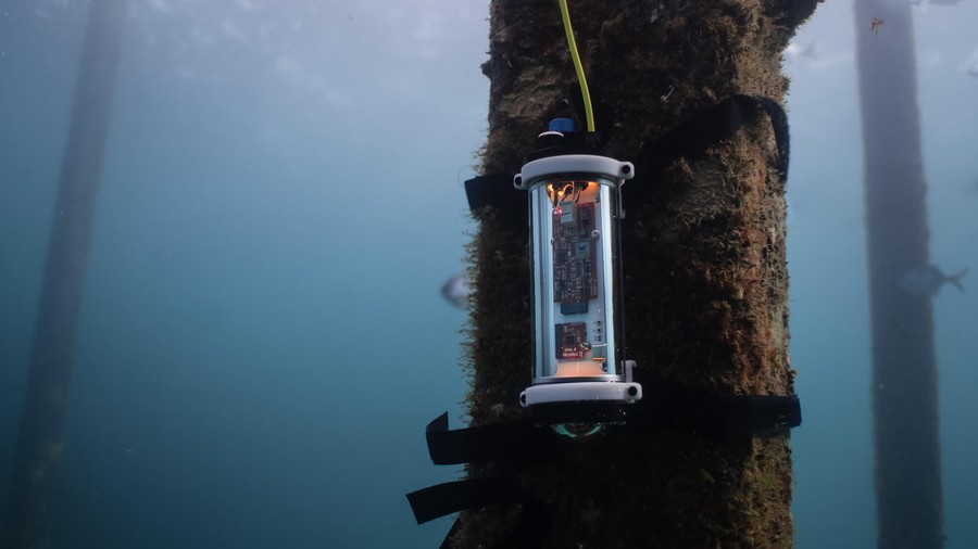
This write-up summarises my (successful) attempts at building a Power over Data Line (PoDL) compliant device and power supply as part of a one-month 'sink or swim' approach to designing and testing new hardware, and getting to look at maturity of the 10Base-T1 ecosystem.
I'll quickly cover some PoDL basics, then walk through the critical design decisions and test process for a prototype underwater sensor node suitable for ocean research.
All project files and full schematics are available on GitHub.
Why is Single Pair Ethernet interesting?
Put simply, it's a step closer to what sounds like my ideal transport:
- Supports reasonably high data rates (for microcontrollers) at ~10 Mbps,
- Adds the ability to provide reasonable amounts of power with up to 50W,
- Has the ability to integrate easily with existing networking stacks,
- and doesn't over-complicate wiring.
As a bonus, Single Pair Ethernet supports long range >1km cable runs which exceed typical Ethernet specifications, and does so while aiming for far lower power consumption.
Off to the side, 10Base-T1S has similar goals but is built around a multi-drop half-duplex wiring configuration for shorter distance networks.
Power over Data Lines
With conventional PoE, two spare pairs are used for power transfer which avoids the need to mix power and data.
With SPE+PoDL, the high frequency data signals are low voltage (1.0Vpp or 2.4Vpp) compared to the large DC offset required by PoDL. Add in the fact that a single cable run can be >1km long and some care needs to be taken to correctly couple and decouple data from the power lines.
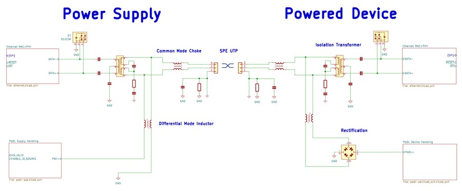
The coupled inductors (differential mode) couple DC supply onto the twisted pair, while the transceiver's data is inductively coupled through the isolation transformer. To reduce common mode noise, a choke filters the input, and it's also a good idea to protect the transceiver from high voltage transients with suitable ESD supression measures (typically TVS diodes).
For convenience in the field, the specification allows the conductors to be installed in any orientation. This means that downstream devices need to support reverse polarity power with a rectification or FET based switching arrangement.
PoDL Types and Classes
Standards develop and change over time as the group and industry work out the details. SPE+PoDL is just as confusing as I expected and has 16 supported power classes and a compatibility matrix between power classes and 10Base-T1S, 10Base-T1L, 100BaseT1, 1000BaseT1.
IEEE 802.3bu started by defining several Types of power capable SPE devices A, B, C and D, primarily for automotive use. This included 10 classes for unregulated and regulated 12V and 24V options, along with regulated 48V.
| Class | PD Power Budget (W) | PD Vmin | PD Vmax | Current Limit (mA) |
|---|---|---|---|---|
| 0 | 0.5 | 4.94 | 18 | 101 |
| 1 | 1 | 4.41 | 18 | 227 |
| 2 | 3 | 12 | 18 | 249 |
| 3 | 5 | 10.6 | 18 | 471 |
| 4 | 1 | 10.3 | 36 | 97 |
| 5 | 3 | 8.86 | 36 | 339 |
| 6 | 5 | 23.3 | 36 | 215 |
| 7 | 10 | 21.7 | 36 | 461 |
| 8 | 30 | 40.8 | 60 | 735 |
| 9 | 50 | 36.7 | 60 | 1360 |
IEEE 802.3cg later simplified things by adding Type E devices (10Base-T1L only) and another 6 classes of power delivery suitable for ~1-8W devices running with 20-30V (nominally 24V), and a massive 50W when using 54V supplies.
| Class | PD Power Budget (W) | PD Vmin | PD Vmax | Current Limit (mA) |
|---|---|---|---|---|
| 10 | 1.23 | 14 | 30 | 92 |
| 11 | 3.2 | 14 | 30 | 240 |
| 12 | 8.4 | 14 | 30 | 632 |
| 13 | 7.7 | 35 | 58 | 231 |
| 14 | 20 | 35 | 58 | 600 |
| 15 | 52 | 35 | 58 | 1579 |
For my typical projects, being able to use 24V with a few watts of power budget is the right balance of capable and practical, so I decided to aim for Class 12 support.
When a power supply wants to provide power to a downstream device, it first attempts to detect compliant PD hardware, and then uses a bidirectional communications process called SCCP to classify the device.
Detection & Classification
Detection is reasonably straightforward - the power supply uses a constant-current source capable of 9-16mA and ensures the open-loop voltage doesn't exceed 5.5V.
The downstream device uses this stimulus current to power up a small regulator for it's VID circuitry. Then, it sinks current until the voltage is brought within the specified signature range of 4.05-4.55V.
The power supply monitors the power line voltage and can signal to when a valid downstream device is identifying itself correctly.
The classification process is more involved, where both sides implement current sinking circuitry for a half-duplex 333bps communications link. The TI SNLA395 appnote explains it reasonably well.
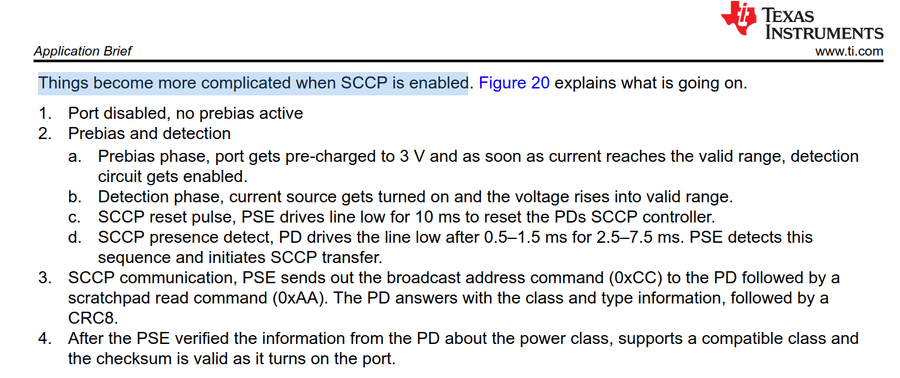
Electrically this can be as simple as some resistors and an extra mosfet on each board controlled by a microcontroller, but reference material often includes extra buffering and input protection circuitry.
While literature suggest either bit-banging or an SPI peripheral make data transfer easy, I wasn't particularly keen to spend several hundred dollars to buy the specification and then implement a driver to communicate correctly.
Looking for alternatives, the Analog Devices LTC9111 is a viable option for adding SCCP to the Type E downstream devices, with the added benefit of simplifying input polarity handling. For ~$5 and a simplified BOM this is probably a pretty easy choice.
Unfortunately, a simple supply-side SCCP controller doesn't seem to exist yet, the only option I could find was the incredibly expensive ($20) LTC4296 5-port controller intended for switch style devices.
Fast Startup
For a fully capable PoDL supply, both detection and classification steps would be implemented.
However the standard allows us to only implement detection OR classification and call it 'Fast-start operation'. Given the lower complexity of detection, this was a pretty appealing option.
Submersible Sensor Node
So now we understand what SPE+PoDL will let us do, lets get into the design.
Marine scientists often need to make observations or stimulate the environment. The combination of harsh environmental conditions, specialised hardware, and tricky cross-domain skill-sets needed to develop bespoke hardware presents a special challenge.
Did you know: Playing sounds of healthy reefs can help attract marine life to damaged reefs and accelerate recovery processes!
A single conductor pair providing power and data over long distances offers some interesting improvements in data rate, reduced power consumption, and simpler (cheaper/lighter) cabling.
Building on the Sparkfun MicroMod ecosystem (and hardware provided as part of the design challenge), I'll design replacements for the data-only ADIN1110 function boards which add PoDL capabilities.
Then we'll package them in a waterproof enclosure suitable for small sensing payloads as a technology demonstrator.
Mechanical Design
The electronics need to fit inside a practical waterproof housing, so I let the mechanical design drive the design choices for the electronics stack.
I considered building a housing out of PVC pipe with glands and a heaping of potting compound, but found BlueRobotics sell reasonably configurable waterproof housing parts for building custom modules for use on their ROV platforms. As a bonus, STEP models for most of their parts made it pretty easy to plan out the housing and mock up the electronics.
I chose the smallest 2″ acrylic tube (~58mm OD) and matching aluminium end-caps. This provides an internal volume constrained by the 50 mm tube diameter and ~118 mm maximum gap between bulkheads.
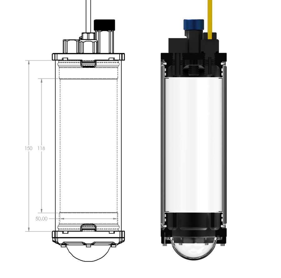
The top cap/bulkhead has 4×M10 threaded holes for accessories as part of BlueRobotic's hardware ecosystem. The prototype uses:
- 4.5mm Wetlink penetrator for the tether cable
- 10m, high resolution pressure sensor
- White indicator LED
- Pressure relief/test valve
Whilst this prototype won't see properly deep water, BlueRobotics suggest this tube configuration should be capable of withstanding 200 meter operation, and far deeper if an aluminium sleeve is used.
I created mockup PCB models which I could use for board outlines in KiCAD, and to check how much height was available for the tall parts like SPE connector block and inductors.
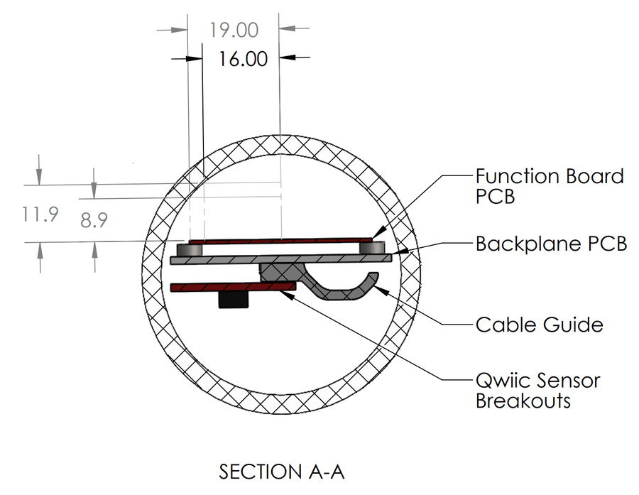
There's a reasonable amount of room in the tube, but clearances like these usually have a habit of looking larger when being designed on a screen.
There are 3 PCB's that need to be designed - the main 'spine' PCB which behaves like a MicroMod compliant carrier board, and the power supply and device variants of the SPE+PoDL communications board.
Backplane PCB
Acting as the MicroMod 'carrier', this board acts as the tube's electrical spine and provides the processor and function board NGFF (aka M.2) connectors, as well as USB and SWD connectors, a 3.3V regulator, some I2C headers, and breakout pads for expansion IO.
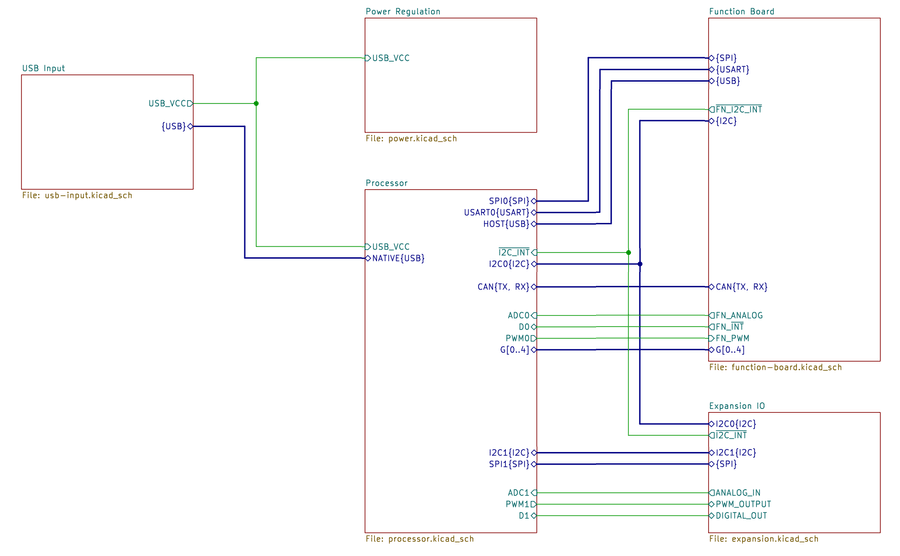
The hardest part of designing this board was trying to untangle the supported GPIO across the range of processor boards, and how that's mapped against the function boards. While Sparkfun's documentation and guides normally sit between 'pretty good' and 'excellent', this process was rather tedious.
From another (unfinished) project, I already had pretty much the entire range of MicroMod processor boards laying around (ESP32, STM32F405, NRF52840, RP2040, SAMD51, Teensy, Apollo3/Artemis) and wanted the design to support the widest range of targets possible (the whole point of MicroMod).
This list of options is cut down substantially if much more than the primary SPI and I2C busses are needed, you want ADIN1110 example library to work, and most processor boards have subtle implementation inconsistencies which turn the pin allocation into a trade-off balancing act.
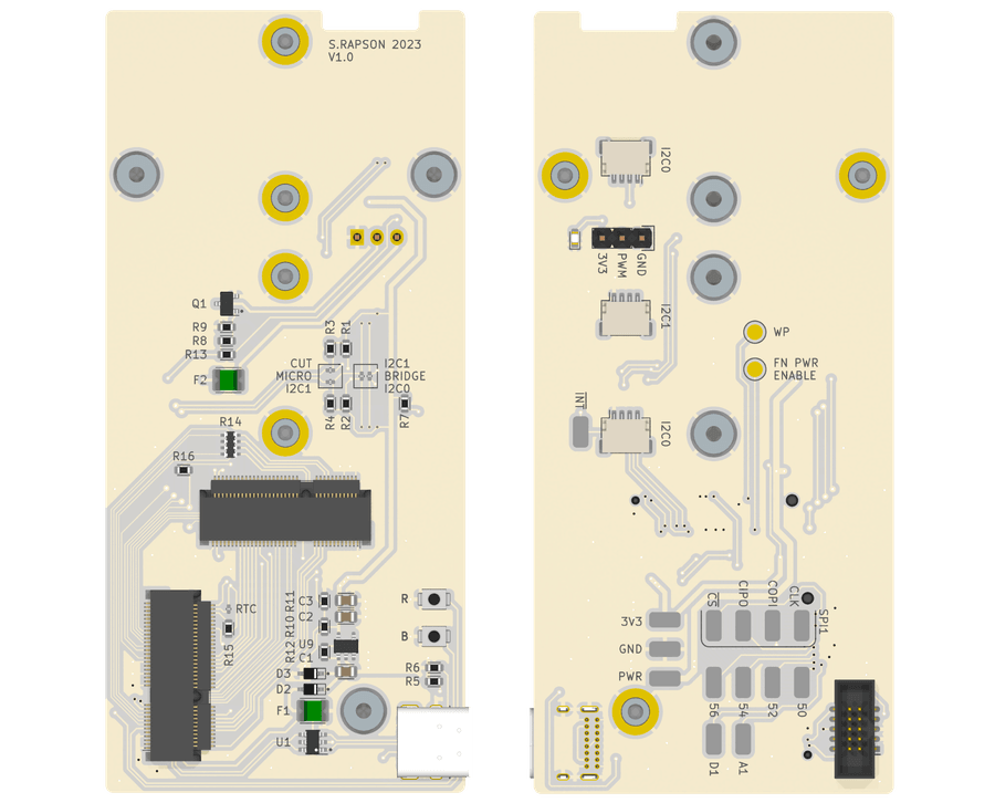
It's a two-layer, 1.6mm, 46 x 100 mm board with pretty relaxed fabrication requirements, costing under $10 from typical commodity Chinese PCBA fabs.
I opted to try the taller 4mm solderable standoff on the rear for sensor mounting and added some spare IO pads and solderable links to make/break the I2C1 bus from the connectors.
PD Function Board
This function board implements the ADIN1110 SPE transceiver in a similar manner to Sparkfun's function board, but deviates from the dev-kit by adding the necessary coupling network and detection circuitry to act as a Class 10-12 PoDL device aka PD.
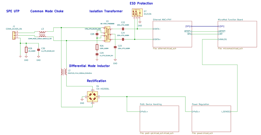
I won't go into the implementation details around the ADIN1110 or MicroMod edge-connector, but if you're interested the full schematics are in the Git repository.
The key areas of discussion are the signature circuitry, and how power is handled once the supply enables full bus voltage.
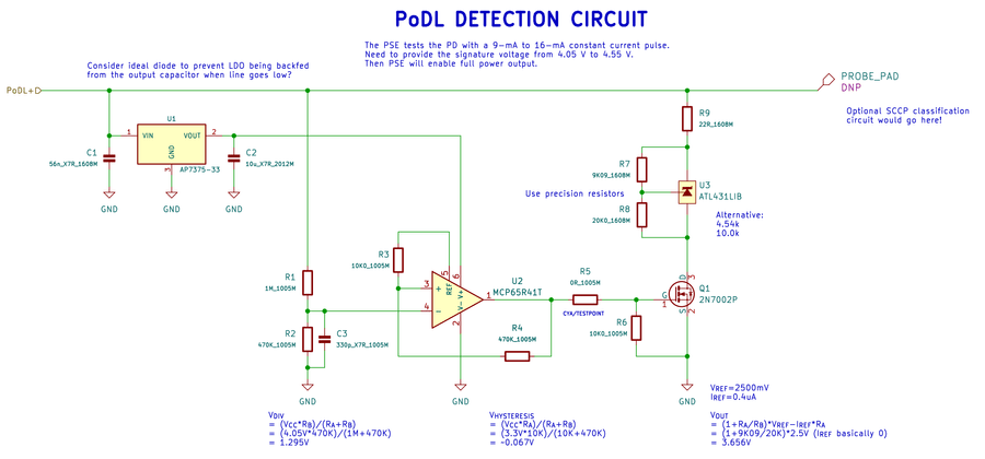
From left to right, we've got a AP7375 wide input voltage LDO which can tolerate bus voltage providing the 3.3V supply to a MCP65R41T comparator with an internal 1.2V internal reference.
The voltage divider (R1, R2) is configured to output approximately 1.2V (matching the internal reference voltage) for a 4.05V input voltage. The output of the comparator then controls a simple N-channel mosfet which switches the TL431 shunt regulator on or off, resulting in a regulated voltage which matches the signature voltage range.
In bench testing the signature voltage measured on the supply side was ~3.905V, slightly lower than intended.
I ended up replacing
R2with 390k to compensate for voltage drop over the rectifier diodes, resulting in a signature voltage of 4.4V.
Assuming the detection circuit works correctly, the power supply would then enable the full bus voltage of 24VDC.
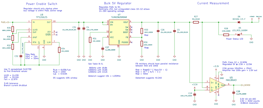
The TPS26625 eFuse switch is configured to automatically switch on once the input voltage is above the PoDL Class 10-12 minimum voltage specification of 14V. It also provides configurable over-voltage and current limiting which makes a compact layout possible.
The 5V regulator is an interesting part - the Texas Instruments TLVM23625 is a tiny, 36V capable, 2.5A switch-mode regulator with an integrated inductor and switch. This was pretty helpful with the constrained layout.
The 5V output is used to power the function board's 3.3V LDO, and also back-powers the carrier board. I included a current shunt and amplifier allow for sink-side current measurement on the 5V rail.
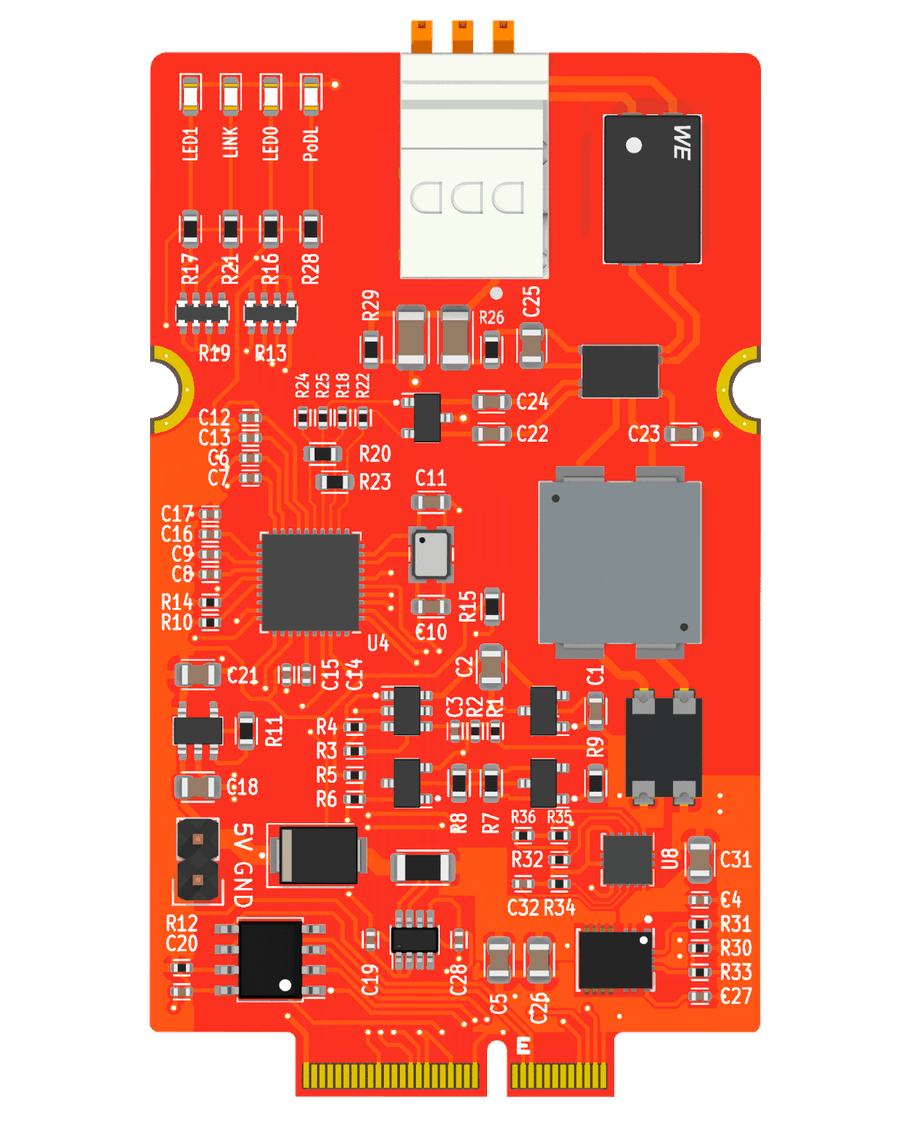
The resulting layout is reasonably dense, but maintains the same MicroMod Function board dimensions.
I tweaked the 5V regulator's feedback network after testing. I was seeing the intended 5.03V regulated voltage, but needed to compensate for the ~0.205V drop over the protection diode.
PSE Function Board
This board shares the input coupling network and ADIN1110 design with the PD board, but replaces the detection signalling circuitry and bulk regulator with the necessary circuitry to test and detect valid downstream devices. Instead of using the power switch to power up the board when bus voltage is within spec, it's used to switch the HV input on once detection succeeds.
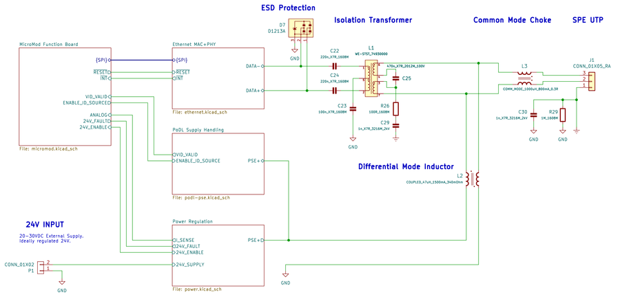
Unlike the PD board, managing the detection process does require microcontroller interaction to enable the current source, watch the detection circuit, and then disable the current source before enabling the HV switch.
Additionally, maintain full voltage signature (MVFS) behaviour needs the microcontroller to monitor the current sense signal for a minimum peak load of 11mA per 10ms span to keep the power supply active (though this can be set lower if needed).
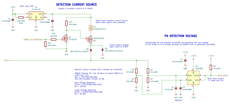
From left to right, a 7V output wide input LDO powers the current stimulus circuit. Instead of building a constant-current source from scratch, I use a NSI50010YT1G LED driver IC which is switched on/off by a P-channel mosfet. This approach is intentionally simple, but probably not ideal as there's limited control over the current output and startup slew-rate.
The current source output is protected from the switched 24V output by a diode, and also has a 5.6V zener diode to clamp the output voltage to the specified maximum open-loop voltage of 5.5V.
Once the downstream powers up and starts presenting the signature voltage range of 4.05V to 4.55V, the TLV6700 window comparator output provides the microcontroller with the VID_VALID signal.
The microcontroller then enables this board's TPS26625 eFuse to pass the 24V input supply to the downstream device. On this board, the eFuse's ULVO and OVP is configured for the Class 10-12 allowable PSE range of 20-30V.
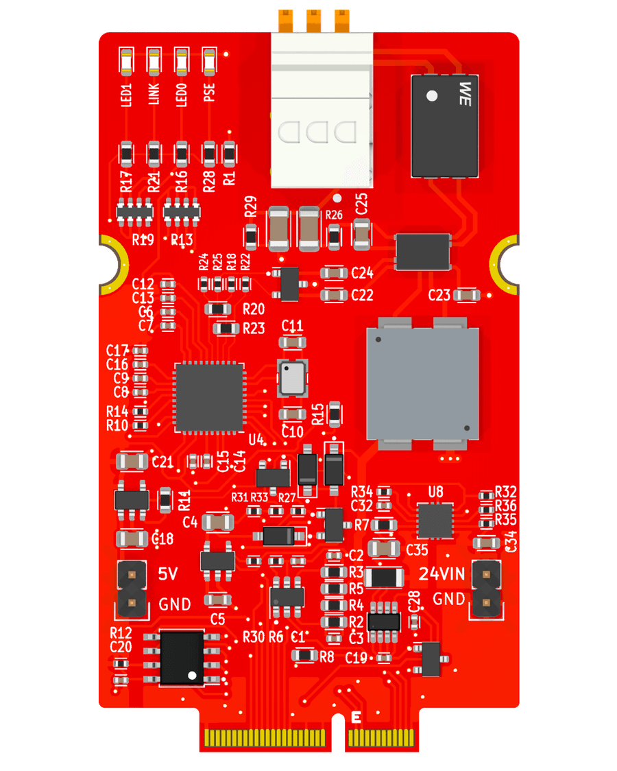
I'm a little annoyed with how the detection circuitry part placement and routing turned out, a mix of rushing the design late at night and higher part count made it tricky to fit in the same area as the PD's circuitry.
As an aside, this PSE design probably makes more sense as it's own carrier board, or as a media converter to 10BaseT ethernet.
Implementing it as a function board allowed for design re-use and opens up some flexibility in final use-cases though.
Printable mounting brackets
With the boards designed, I brought exported STEP models back into my CAD model and designed a pair of 3D printed board mounts use the 4×M3 internal mounting holes in the bulkheads.
The upper bracket abuses the solderable standoffs on the rear of the backplane board as mounting features, along with the key cutout in the PCB to force alignment.
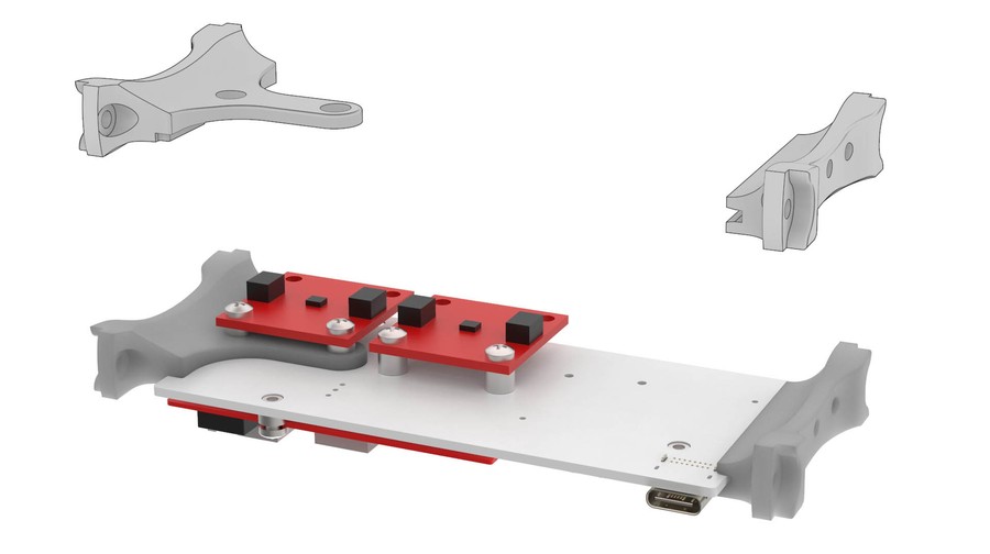
Because the mounted electronics need to slide through the tube to meet the other end-cap, a simple tapered groove design is used to retain the PCB once installed.
Electronics Assembly & Testing
PCBs and printed parts were ordered from China and arrived in South Australia in a pretty impressive 4-days. The components from DigiKey arrived a day or two later.
I assembled 2 of each board using a pretty typical paste stencil and reflow plate, with some hot air assisting for heavier parts.
Bring-up testing didn't throw any surprises, I started with a lab supply to check the power paths didn't have any critical errors.
The PD board eFuse ULVO/OVP behaviour and 5V regulator behaved as expected. The rectifier and decoupling network also handled 24V with either polarity without issue, dropping about 0.4V across the rectifier diodes.
Testing the PSE board was similar, checking the current source output with a multimeter, then using the lab supply to provide a 4.2V test voltage to trigger the window comparator's output.
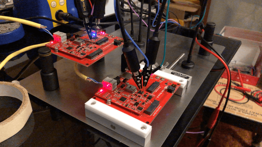
I quickly wrote some simple PD detection handling code which uses a state-machine to control the detection behaviour:
- Enable the current source,
- Wait for the downstream device to boot,
- Check the comparator output for VID valid flag (and filter it),
- Disable the current source, wait a bit,
- Enable the power switch to enable 24V supply.
The scope trace below shows the PoDL bus voltage in yellow (CH1), and the PD board's 5V regulator is the blue trace (CH2). The state-machine timing was intentionally slowed down to make the trace easier to understand.
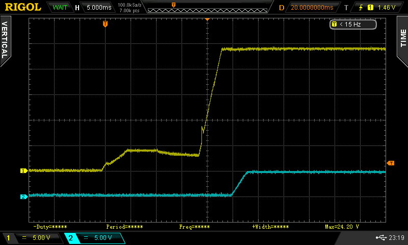
We can see the current source enable, settle at 4.4V for 5ms, then decay once the current source is disabled. Then the 24V switch enables with a nicely controlled slew rate thanks to the eFuse, followed by the 5V regulator cleanly coming up a couple of milliseconds later.
This is a successful power up sequence for 24V PoDL!
On the data side, I mounted the custom function boards into the MicroMod function carrier and flashed some basic Arduino test sketches to exercise the ADIN1110's self-test loopback.
Adin1110 found!Frame Generator/Checker Results: (FG) Sent: 20000 frames (FC) Received: 20000 frames Rx Errors = 0 LEN_ERR_CNT = 0 ALGN_ERR_CNT = 0 SYMB_ERR_CNT = 0 OSZ_CNT = 0 USZ_CNT = 0 ODD_CNT = 0 ODD_PRE_CNT = 0 FALSE_CARRIER_CNT = 0We can communicate with the MAC over SPI successfully, so that part of the implementation is also working fine!
Making late night mistakes
At this point, it's rather amazing that the design and implementation has gone almost perfectly to plan...
So I tried testing a 6S LiPo battery as my 'field' 24V source instead of my lab supply. I'm sure a few of you reading are seeing where this is going.
The inrush spike resulted in the PSE board's onboard (unprotected) 7V LDO being sacrificed to the cause. Hindsight is 20/20 and immediate, so I cobbled together a simple resistor based soft-start circuit and filter from scrap parts to prevent any future mishaps.
Also, it was about this time when I noticed I had unfortunately placed the processor board mounting standoff about 1.05mm further than it's intended position. Not a big deal, but incredibly frustrating to see gap between screw and board edge.
Firmware
With the electronics mostly working without issue, it was time to interface to the test sensors and send some packets.
The boards were designed without assuming any specific sensors would be used, but I used these I2C sensors:
- Temperature & Humidity -
SHTC3via SparkfunSEN-16467 - Motion -
LSM6DSOvia SparkfunSEN-18020 - Depth/Pressure -
MS5837via BlueRoboticsBar02
The Sparkfun breakouts mount directly to the standoffs on the rear of the backplane board.
The Bar02 comes with a JST-GH connector, so I re-terminated it with a JST-SH connector for consistency with the other boards and headers on the backplane PCB.
Attempting to avoid any more scope-creep, I opted to use the Arduino ecosystem instead of going bare-metal with my preferred STM32 or ESP32 toolchains. The promise of quick integration with pre-made libraries for the sensors, T1L transciever, and communications protocol was alluring.
The project is structured as a simple super-loop which runs some state-machines to handle polling sensors before packing data into packets for transfer over SPE.
Writing a MS5837 Driver
The very cool MS5837-02 pressure sensor supports absurdly high precision (via oversampling) at rather high sample rates - starting with a base resolution of 0.11 mbar at 1.5kHz and 0.016 mbar at ~60Hz.
Converting the pressure resolution into a more understandable unit puts the absurdity of this sensor into context:
0.016 mbarequates to a depth change of roughly0.16 millimetersin sea water.160 μm!
Unfortunately, the BlueRobotics Arduino driver only supports the maximum oversampling (OSR = 8192) setting and forces a 40ms blocking delay...
I implemented a generic C library to work with the MS5837-02, letting the integrating developer take back some control over configuration and sampling behaviour. This approach allows the library to be used with a simple state-machine or with RTOS style yields.
// FreeRTOS example taskuint16_t wait_us = 0;// Measurement request function returns a microsecond duration// which we need to wait out before attempting to read the sample.// Request a pressure readingwait_us = ms5837_start_conversion( &sensor, SENSOR_PRESSURE, OSR_8192 );vTaskDelay( pdMS_TO_TICKS(wait_us/1000) );ms5837_read_conversion( &sensor );// Request temperature readingwait_us = ms5837_start_conversion( &sensor, SENSOR_TEMPERATURE, OSR_2048 );vTaskDelay( pdMS_TO_TICKS(wait_us/1000) );ms5837_read_conversion( &sensor );// Once pressure and temp are sampled, run the conversion functionms5837_calculate( &sensor );float pressure = ms5837_pressure_mbar( &sensor );float temperature = ms5837_temperature_celcius( &sensor );While the temperature is needed for the 2nd order pressure compensation maths, I didn't see any downside from reducing the temperature oversampling slightly which also allows for quicker turnaround time.
My driver is a simple open-sourced and available standalone on GitHub.
Internal Sensors
The SHTC3 and LSM6DS0 Arduino libraries were better behaved, and I was able to throw together a reasonable implementation sampling the IMU's FIFO buffer reasonably easily.
ADIN1110 Serial Bridge
At the start of the project I wanted to implement proper TCP/IP support via LwIP to connect the sensor node directly to a normal Ethernet network through a media converter, but the lack of integration examples and diminishing amount of time meant I knew I would run out of time during debugging. Maybe next time!
Building off Sparkfun's reasonably thin sfe_spe_advanced wrapper around Analog Device's library, I was able to send raw buffers of bytes between the transcievers with fairly minimal effort.
Because I'm familiar with the protocol (and wrote the library) I was able to connect the electricui-embedded read and write callbacks, and setup the power-supply side MicroMod process to act as a nearly transparent SPE-to-Serial proxy.
The fact that a 10 Mbps networked node was constrained by a 10x slower serial link (
912600 baud) was slightly amusing, but will hopefully be an area I can address with a bit more time in the future.
User Interface
I'm using Electric UI's DataFlow and DataTransformer system to calculate real-time wave height statistics on the stream of depth sensor data. Turns out wave analysis and meaningful visualisations are slightly non-trivial, so I'll probably write a second post going into greater depth.
As a quick overview:
- Filter the incoming pressure measurement stream to reduce noise,
- Calculate the rate of depth change (derivative),
- Detect peak and troughs, and the time between them,
- Average the midpoint height of detected waves to create a long-running reference depth,
- Generate a histogram to show wave behaviour relative to the reference depth.
These statistics are data-loggable alongside the raw sensor streams.
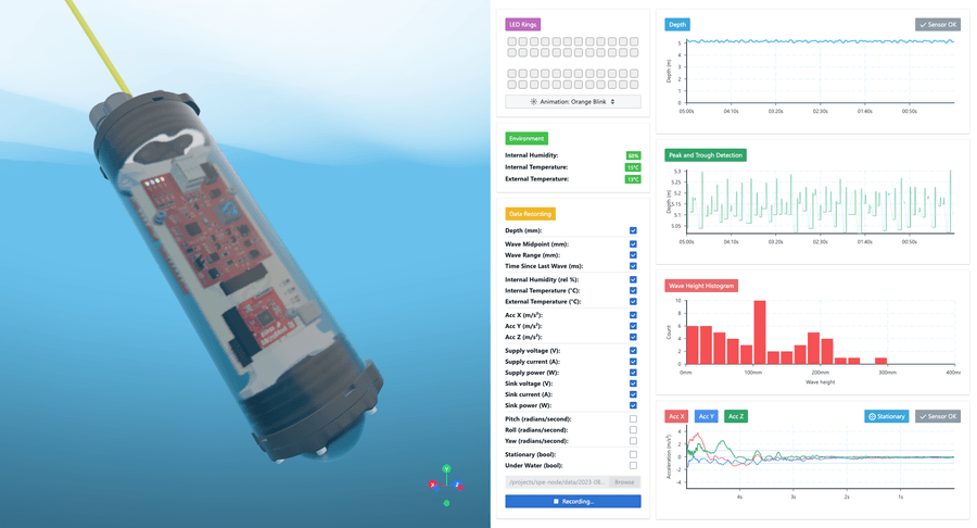
Thanks to reasonably easy export from the CAD packages, we have a high quality 3D model of the tube and custom electronics just sitting there...
A quick trip through Blender to perform Planar Decimation helps bring the model complexity down from ~2M tris to a couple hundred thousand, and we export the file as a gltf.
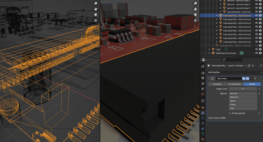
It's pretty easy to then import and use with ThreeJS.
Final Assembly
With firmware running and the boards finished, it was time to mount the PoDL PD function board, ESP32 MicroMod processor, and internal sensor breakouts to the backplane board.
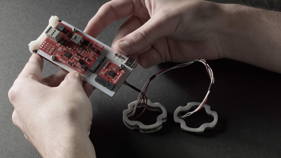
Also pictured is the vanity APA102-2020 LED rings which were intended to act as an adjustable mock load to test the power delivery components.
The printed mount was then screwed to the aluminium cap, where I had already installed the 2-core tether cable and external sensors.
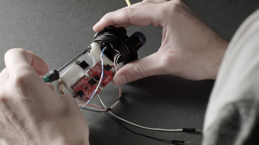
After a bit of cable management, the assembly was suspended in the acrylic sleeve and the bottom cap carefully aligned to retain the backplane PCB.
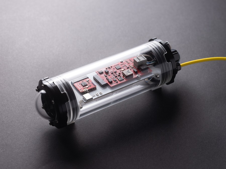
Once assembled, I removed the pressure-relief valve stem and attached a vacuum pump to perform a leak test.
Overall, I'm pretty happy with how everything turned out, just wished I had a bit more time for refinement!
Field Testing
We tested the tube in a pool briefly to check buoyancy. During the early mechanical design stages I created a simple spreadsheet to estimate the assembly mass and displacement from first-principles which suggested additional ballast weight was not needed (slightly negatively buoyant). In the real-world it was slightly positively buoyant and could use a bit of extra weight.
Being the natural over-achiever (and qualified diver) that he is, my colleague Michael suggested we should give it real-world test.
We drove down to a popular dive reef with good jetty access to test the sensor node.
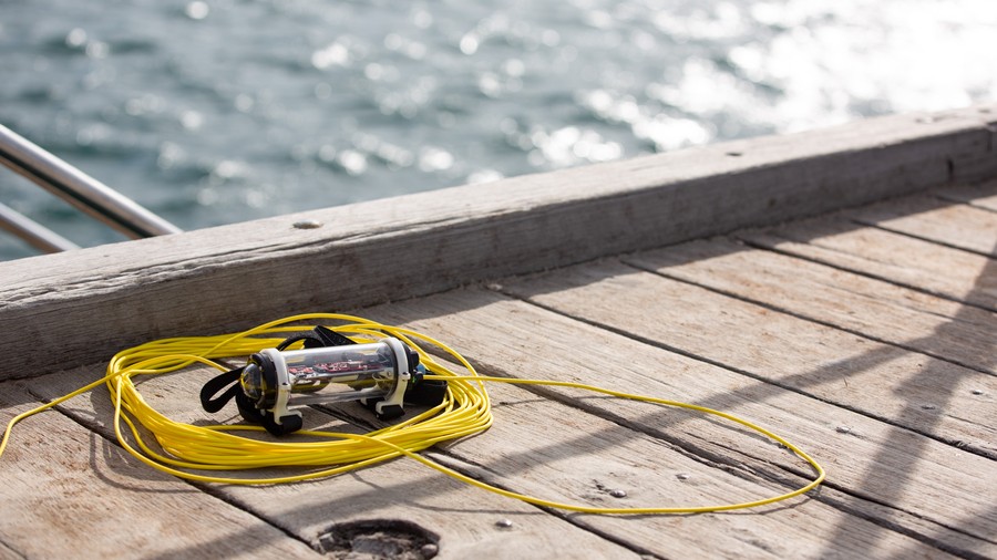
By stitching some velcro lengths to each side of some printed mounting clamps, it provided a fairly easily removable and non-invasive mounting solution that could be handled underwater.
If the sensor node was deployed for longer periods of time, a more carefully designed mount would be necessary.


I think we got the tick of approval from the locals.
Useful Resources & Thanks
Firstly, thanks to Jack & Brittany for accompanying us during the test dive. It wouldn't have gone as smoothly without you!
Thanks to Michael for doing such a great job documenting the assembly and test.
On the design side, I found these manufacturer app notes helpful:
- TI SNLA395 - How to Implement an IEEE 802.3cg or 802.3bu-Compliant PoDL PSE
- TI SNVAA25A - 10BASE-T1L Power over Data Lines Powered Device Design
- TDK - How to implement 10Base-T1L
There was also a good discussion on HackerNews.